Silicon Genesis Broadens the Use of Layer Transfer Methods for Advanced CMOS Image Sensor Stacks
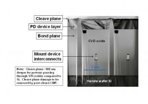
Silicon Genesis has extended its NANOCLEAVE Layer Transfer (LT) methods for use in 3DIC device stacking to make high bandwidth CMOS Image Sensor (CIS) devices
3D stacking methods have been a foundational technology of advanced CIS fabrication for over a decade, using bonding and mechanical grinding die thinning for photodiode, memory and signal output device layers. However, mechanical grinding methods present strong limitations for film thickness dimensional control for device layer thicknesses less than 20um due to injecting internal stresses leading to multiple device issues, such as recombination leakage currents and increased refresh cycles for active memory layers. Mechanical grinding also leads to yield loss in 3D stacks due to die edge cracking and limitations of the achievable scale of multi-layer stacking.
Following its earlier success with 3DIC Mega-pixel CMOS BSI Image Sensors, SiGen is collaborating with partners to apply its NANOCLEAVE process to multiple layer CIS products designed to incorporate beyond three and four layer stacks.
For advanced CIS elements stacked with high-speed signal processing CMOS, the result is a unique combination of multiple layer photo diodes for improved quantum efficiency and light capture, high speed processing, global shutter capability, high frame rates and long-term operational reliability. These new CIS products will be many generations ahead of current CIS processors in the market.
By achieving an active layer thickness of 2um or less, with cross-wafer thickness uniformity of less than 100nm, SiGen’s device layers are two to five times thinner than can be reliably achieved with temporary bond, grind back and etch methods. Also, when compared to interposer stacking using 2.5D packaging methods, the SiGen approach provides an order of magnitude higher signal bandwidth from the use of shorter and denser vertical TSV and metal signal connections, as well as much improved thermal conductivity throughout the atomically bonded stack layers.
Another advantage of SiGen layer transfer methods is that with the addition of precision aligned wafer bonding and room temperature cleaving tools, 3DIC system stacking can be achieved with the standard transistor formation and metal interconnect tool sets in present day IC fabrication foundries. This is without dependence on mainstream 2.5D and 3D packaging formats and opens up new avenues for 3DIC design and fabrication.
CIS layer transfer technologies with the SiGen NANOCLEAVE process for wafer-scale bonding and cleaving further advances device layer transfer methods for 3DIC. These new methods enable broader applications for stacking and cross-die interconnect technologies of diverse wafer and die-scale devices for heterogeneous integration of 3DIC systems.
SiGen continues working in close collaboration with its customers for 3DIC technology development, transfer, licensing, and equipment sales, resulting in reduced cost, higher performance and improved quality multi-layer stacked 3DIC devices.
About Silicon Genesis
Silicon Genesis is a leading provider of engineered substrate process technology and equipment for the semiconductor, display, and optoelectronics markets. SiGen’s technology is used for production of Silicon-on-Insulator (SOI) semiconductor wafers and 3DIC stacks of CMOS device layers for high performance applications. SiGen develops innovative substrates through thin-film and thick-film engineering, enabling new applications and markets for its customers. SiGen's customers and partners include top players from substrate, device and equipment suppliers throughout the world. Founded in 1997, SiGen is headquartered in Fremont, California. For more information, visit www.sigen.com for the complete SiGen NanoTec offerings of layer transfer process, equipment technology and services.
Theodore Fong
Silicon Genesis Corporation
email us here
EIN Presswire does not exercise editorial control over third-party content provided, uploaded, published, or distributed by users of EIN Presswire. We are a distributor, not a publisher, of 3rd party content. Such content may contain the views, opinions, statements, offers, and other material of the respective users, suppliers, participants, or authors.


